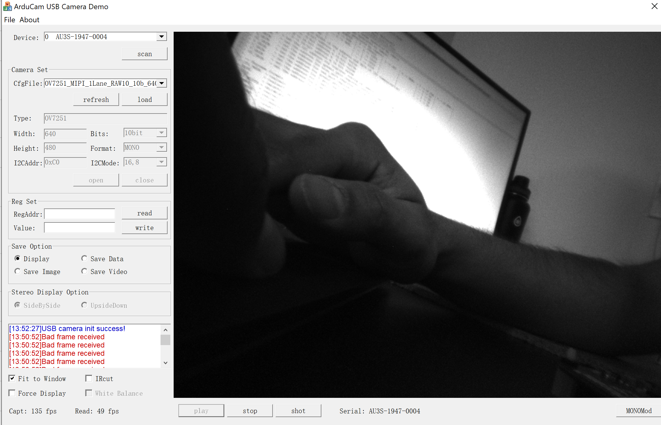
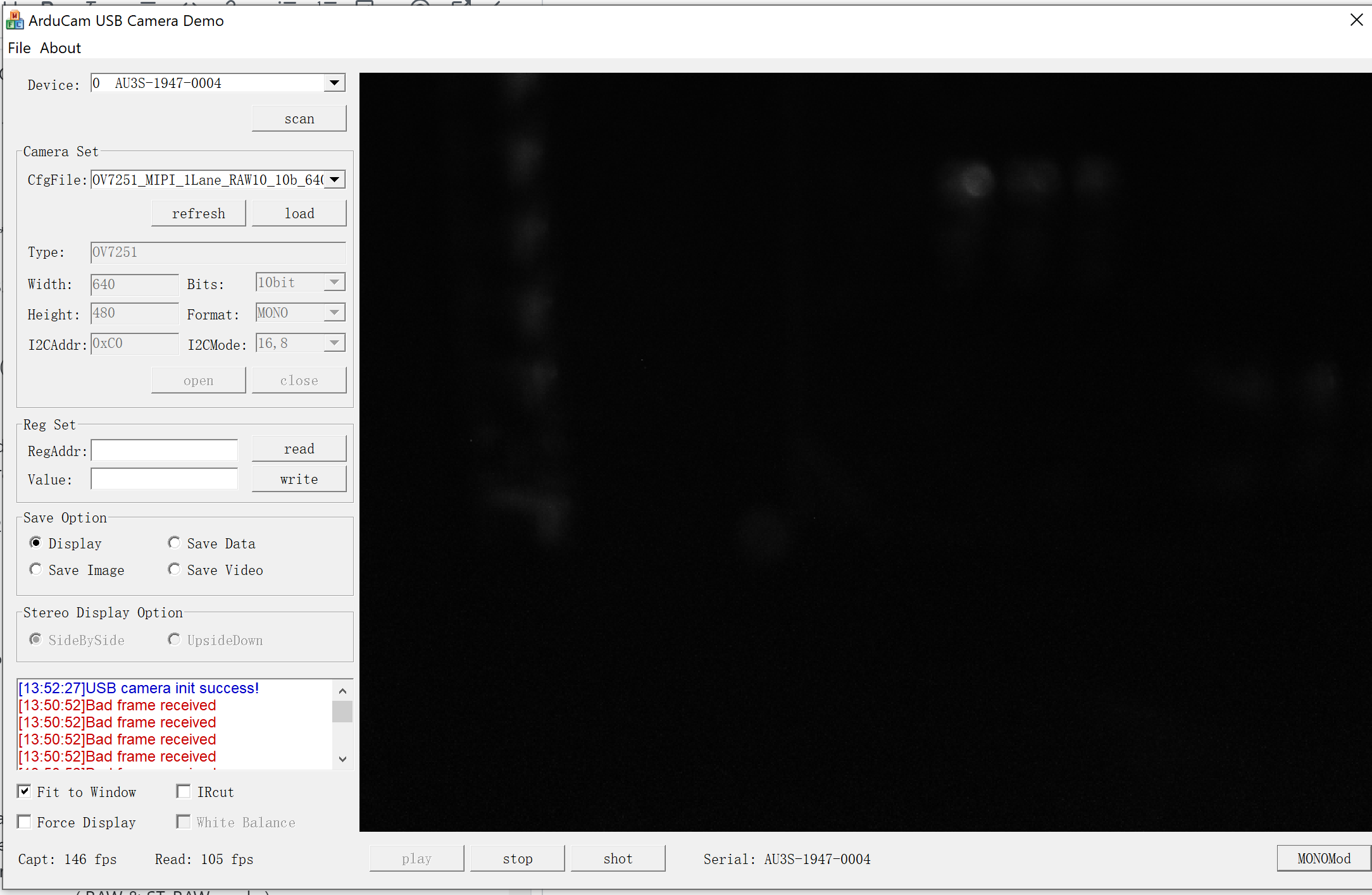
**The components I am using for my Arducam are UC 545 Rev.C(OV7251) camera, UC-489 Rev.C MIPI adaptor, andUC-425 Rev.C USB shield. Normally, read shows 49 fps, but when an object brought very close to the camera the read goes over 100 fps. I want the 'read' to be stable around 130fps. I have attached the pictures and cfg files below. **
;**************************************************************************************/
; ----- camera parameter -----
; [camera parameter]	Camera parameter set for USB2.0 & USB3.0 mode
;
; -- Keyname description:
; CFG_MODE  = set the config mode for camera: 0 -> User define(UI)
;											  1 -> This config File
; TYPE      = set the name of the camera module
; SIZE		= set the width and height of the image generated by camera
; BIT_WIDTH = set the bit width of the image generated by camera
; FORMAT    = set the format of the image generated by camera:
;				| 0 -> RAW	  | 1 -> RGB565  | 2 -> YUV422   | 3 -> JPG  | 4 -> MONO  | 5 -> ST_RAW	| 6 -> ST_MONO |
;				| -- 0 -> RG  | -- 0 -> RGB  | -- 0 -> YUYV  |           | 			  | -- 0 -> RG  | 			   |
;				| -- 1 -> GR  | -- 1 -> BGR  | -- 1 -> YVYU  |           | 			  | -- 1 -> GR  | 			   |
;				| -- 2 -> GB  |              | -- 2 -> UYVY  |           |			  | -- 2 -> GB  |			   |
;				| -- 3 -> BG  |              | -- 3 -> VYUY  |           | 			  | -- 3 -> BG  | 			   |
; I2C_MODE  = set the bit width of the address and data of I2C communication:
;				0 ->  8 bit address &  8 bit value
;				1 ->  8 bit address & 16 bit value
;				2 -> 16 bit address &  8 bit value
;				3 -> 16 bit address & 16 bit value
; I2C_ADDR  = set the I2C address for register config of camera
; G_GAIN    = set the address for green1_gain register config of camera	( RAW & RGB565 & ST_RAW mode )
; B_GAIN    = set the address for blue_gain register config of camera	( RAW & RGB565 & ST_RAW mode )
; R_GAIN    = set the address for red_gain register config of camera	( RAW & RGB565 & ST_RAW mode )
; G2_GAIN   = set the address for green2_gain register config of camera	( RAW & ST_RAW mode )
; Y_GAIN    = set the address for Y_gain register config of camera		( YUV422 mode )
; U_GAIN    = set the address for U_gain register config of camera		( YUV422 mode )
; V_GAIN    = set the address for V_gain register config of camera		( YUV422 mode )
; GL_GAIN   = set the address for global_gain register config of camera
;
; -- Keyname format:
; CFG_MODE  = <value1>							;<comment>
; TYPE      = <value1>
; SIZE		= <width>, <height>
; BIT_WIDTH = <bitWidth>
; FORMAT    = <value1>[, <value2>]
; I2C_MODE  = <value1>
; I2C_ADDR  = <i2cAddress>
; G_GAIN    = [<page>,] <address>, <minValue>, <maxValue>
; B_GAIN    = [<page>,] <address>, <minValue>, <maxValue>
; R_GAIN    = [<page>,] <address>, <minValue>, <maxValue>
; G2_GAIN   = [<page>,] <address>, <minValue>, <maxValue>
; Y_GAIN    = [<page>,] <address>, <minValue>, <maxValue>
; U_GAIN    = [<page>,] <address>, <minValue>, <maxValue>
; V_GAIN    = [<page>,] <address>, <minValue>, <maxValue>
; GL_GAIN   = [<page>,] <address>, <minValue>, <maxValue>
;
; <valueN>		Index value representing certain meanings
; <width>		Width of the image generated by camera
; <height>		Height of the image generated by camera
; <bitWidth>	Bit width of the image generated by camera
; <i2cAddress>	I2C address for register config of camera
; <page>        Optional address space for this register. Some sensors (mostly SOC's)
;               have multiple register pages (see the sensor spec or developers guide)
; <address>     The register address
; <minValue>	Minimale value of certain address
; <maxValue>	Maximale value of certain address
; <comment>    	Some form of C-style comments are supported in this .cfg file
;
;**************************************************************************************/
[camera parameter]
CFG_MODE  = 1
TYPE      = OV7251
SIZE      = 640, 480
BIT_WIDTH = 8
FORMAT    = 4, 0
I2C_MODE  = 2
I2C_ADDR  = 0xC0

;**************************************************************************************/
; ----- board parameter -----
;[board parameter]					Board parameter set for USB2.0 & USB3.0 mode
;[board parameter][dev2]			Board parameter set for USB2.0 mode
;[board parameter][dev3][inf2]		Board parameter set for USB3.0 mode and USB2.0 interface
;[board parameter][dev3][inf3]		Board parameter set for USB3.0 mode and USB3.0 interface
;
; -- Keyname description:
; VRCMD = set board parameter by vendor command
;
; -- Keyname format:
; VRCMD = <command>, <value>, <index>, <dataNumber>[, <data1>[, <data2>[, <data3>[, <data4>]]]] 		//<comment>
;
; <command>    Value representing certain command
; <value>      value representing certain meanings
; <index>      Index representing certain meanings
; <dataNumber> Number of <dataN>
; <dataN>      Data representing certain meanings
; <comment>    Some form of C-style comments are supported in this .cfg file
;
;**************************************************************************************/
[board parameter]
VRCMD = 0xD7, 0x4600, 0x0100, 1, 0x05
VRCMD = 0xD7, 0x4600, 0x0200, 1, 0x00
VRCMD = 0xD7, 0x4600, 0x0300, 1, 0x40
VRCMD = 0xD7, 0x4600, 0x0400, 1, 0x00
VRCMD = 0xD7, 0x4600, 0x0A00, 1, 0x02
VRCMD = 0xD7, 0x4600, 0x0C00, 1, 0x80
VRCMD = 0xD7, 0x4600, 0x0D00, 1, 0x02
VRCMD = 0xD7, 0x4600, 0x0E00, 1, 0x80
VRCMD = 0xD7, 0x4600, 0x0F00, 1, 0x01
VRCMD = 0xD7, 0x4600, 0x1000, 1, 0xE0
VRCMD = 0xD7, 0x4600, 0x1100, 1, 0x07
VRCMD = 0xD7, 0x4600, 0x2300, 1, 0x03

VRCMD = 0xF6, 0x0000, 0x0000, 3, 0x03, 0x04, 0x0C

[board parameter][dev2]


[board parameter][dev3][inf2]
VRCMD = 0xF3, 0x0000, 0x0000, 0
VRCMD = 0xF9, 0x0000, 0x0000, 0   //8 bit
;VRCMD = 0xF9, 0x0001, 0x0000, 0    //12 bit

[board parameter][dev3][inf3]
VRCMD = 0xF3, 0x0000, 0x0000, 0
VRCMD = 0xF9, 0x0000, 0x0000, 0   //8 bit
;VRCMD = 0xF9, 0x0001, 0x0000, 0    //12 bit

;**************************************************************************************/
; ----- register parameter -----
;[register parameter]					Register parameter set for USB2.0 & USB3.0 mode
;[register parameter][dev2]				Register parameter set for USB2.0 mode
;[register parameter][dev3][inf2]		Register parameter set for USB3.0 mode and USB2.0 interface
;[register parameter][dev3][inf3]		Register parameter set for USB3.0 mode and USB3.0 interface
;
; -- Keyname description:
; REG    = assign a new register value
; DELAY  = delay a certain amount of milliseconds before continuing
;
; -- Keyname format:
; REG    = [<page>,] <address>, <value>             //<comment>
; DELAY  = <milliseconds>
;
; <page>         Optional address space for this register. Some sensors (mostly SOC's)
;                have multiple register pages (see the sensor spec or developers guide)
; <address>      the register address
; <value>        the new value to assign to the register
; <milliseconds> wait for this ammount of milliseconds before continuing
; <comment>      Some form of C-style comments are supported in this .cfg file
;
;**************************************************************************************/
[register parameter]
;DELAY  = 0x100
;REG    = 0x10, 0x00FF
;BITSET = 0x10, 0xF000
;BITCLR = 0x10, 0x8000

REG = 0x0100, 0x00
REG = 0x3005, 0x00
REG = 0x3012, 0xC0
REG = 0x3013, 0xD2
REG = 0x3014, 0x04
REG = 0x3016, 0xF0
REG = 0x3017, 0xF0
REG = 0x3018, 0xF0
REG = 0x301A, 0xF0
REG = 0x301B, 0xF0
REG = 0x301C, 0xF0
REG = 0x3023, 0x07
REG = 0x3037, 0xF0
REG = 0x3098, 0x04
REG = 0x3099, 0x36	//PLL
REG = 0x309A, 0x05
REG = 0x309B, 0x04
REG = 0x30B0, 0x0A
REG = 0x30B1, 0x01
REG = 0x30B3, 0x70
REG = 0x30B4, 0x03
REG = 0x30B5, 0x05
REG = 0x3106, 0x12
REG = 0x3500, 0x00
REG = 0x3501, 0x1F
REG = 0x3502, 0x80
REG = 0x3503, 0x07
REG = 0x3509, 0x10
REG = 0x350B, 0x28  //AEC AGC ADJ
REG = 0x3600, 0x1C
REG = 0x3602, 0x62
REG = 0x3620, 0xB7
REG = 0x3622, 0x04
REG = 0x3626, 0x21
REG = 0x3627, 0x30
REG = 0x3634, 0x41
REG = 0x3636, 0x00
REG = 0x3662, 0x01
REG = 0x3664, 0xF0
REG = 0x3669, 0x1A
REG = 0x366A, 0x00
REG = 0x366B, 0x50
REG = 0x3705, 0xC1
REG = 0x3709, 0x40
REG = 0x373C, 0x08
REG = 0x3742, 0x00
REG = 0x3788, 0x00
REG = 0x37A8, 0x01
REG = 0x37A9, 0xC0
REG = 0x3800, 0x00
REG = 0x3801, 0x04
REG = 0x3802, 0x00
REG = 0x3803, 0x04
REG = 0x3804, 0x02
REG = 0x3805, 0x8B
REG = 0x3806, 0x01
REG = 0x3807, 0xEB
REG = 0x3808, 0x02
REG = 0x3809, 0x80
REG = 0x380A, 0x01
REG = 0x380B, 0xE0
REG = 0x380C, 0x03
REG = 0x380D, 0xA0
REG = 0x380E, 0x02
REG = 0x380F, 0x04
REG = 0x3810, 0x00
REG = 0x3811, 0x04
REG = 0x3812, 0x00
REG = 0x3813, 0x05
REG = 0x3814, 0x11
REG = 0x3815, 0x11
REG = 0x3820, 0x44
REG = 0x3821, 0x00
REG = 0x382F, 0xC4
REG = 0x3832, 0xFF
REG = 0x3833, 0xFF
REG = 0x3834, 0x00
REG = 0x3835, 0x05
REG = 0x3837, 0x00
REG = 0x3B80, 0x00
REG = 0x3B81, 0xA5
REG = 0x3B82, 0x10
REG = 0x3B83, 0x00
REG = 0x3B84, 0x08
REG = 0x3B85, 0x00
REG = 0x3B86, 0x01
REG = 0x3B87, 0x00
REG = 0x3B88, 0x00
REG = 0x3B89, 0x00
REG = 0x3B8A, 0x00
REG = 0x3B8B, 0x05
REG = 0x3B8C, 0x00
REG = 0x3B8D, 0x00
REG = 0x3B8E, 0x00
REG = 0x3B8F, 0x1A
REG = 0x3B94, 0x05
REG = 0x3B95, 0xF2
REG = 0x3B96, 0x40
REG = 0x3C00, 0x89
REG = 0x3C01, 0xAB
REG = 0x3C02, 0x01
REG = 0x3C03, 0x00
REG = 0x3C04, 0x00
REG = 0x3C05, 0x03
REG = 0x3C06, 0x00
REG = 0x3C07, 0x05
REG = 0x3C0C, 0x00
REG = 0x3C0D, 0x00
REG = 0x3C0E, 0x00
REG = 0x3C0F, 0x00
REG = 0x4001, 0xC2
REG = 0x4004, 0x04
REG = 0x4005, 0x20
REG = 0x404E, 0x01
REG = 0x4300, 0xFF
REG = 0x4301, 0x00
REG = 0x4600, 0x00
REG = 0x4601, 0x4E
REG = 0x4801, 0x0F 		//ECC, PH order
REG = 0x4806, 0x0F
REG = 0x4819, 0xAA
REG = 0x4823, 0x3E
REG = 0x4837, 0x19
REG = 0x4A0D, 0x00
REG = 0x5000, 0x85
REG = 0x5001, 0x80
REG = 0x3503, 0x07
REG = 0x3662, 0x03      //RAW8

REG = 0x30B0, 0x08
REG = 0x30B4, 0x06

;REG = 0x5E00, 0x8C      //test pattern bar


DELAY  =  0x10

[register parameter][dev3][inf2]


[register parameter][dev3][inf3]

[board parameter]
;;REM	*********************************************
;;REM	Start up sequence
;;REM	*********************************************
;REM	**************************************************
;REM	TC358746XBG Software Reset
;REM	**************************************************
//REG = 0x0002, 0x0001	//SYSctl, S/W Reset
VRCMD = 0xE1, 0x1C00, 0x0002, 2, 0x00, 0x01
DELAY = 	10
//REG = 0x0002, 0x0000	//SYSctl, S/W Reset release
VRCMD = 0xE1, 0x1C00, 0x0002, 2, 0x00, 0x00

;REM	**************************************************
;REM	TC358746XBG PLL,Clock Setting
;REM	**************************************************
//REG = 0x0016, 0x3077	//PLL Control Register 0 (PLL_PRD,PLL_FBD)
VRCMD = 0xE1, 0x1C00, 0x0016, 2, 0x10, 0x63
//REG = 0x0018, 0x0403	//PLL_FRS,PLL_LBWS, PLL oscillation enable
VRCMD = 0xE1, 0x1C00, 0x0018, 2, 0x04, 0x03
DELAY = 10
//REG = 0x0018, 0x0413	//PLL_FRS,PLL_LBWS, PLL clock out enable
VRCMD = 0xE1, 0x1C00, 0x0018, 2, 0x04, 0x13
//REG = 0x0020, 0x0011	//CLK control register: Clock divider setting
VRCMD = 0xE1, 0x1C00, 0x0020, 2, 0x00, 0x11

;REM	**************************************************
;REM	TC358746XBG MCLK Output
;REM	**************************************************
//REG = 0x000C, 0x0101	//MCLK duty setting
VRCMD = 0xE1, 0x1C00, 0x000C, 2, 0x01, 0x01

;REM	**************************************************
;REM	TC358746XBG GPIO2,1 Control (Example)
;REM	**************************************************
;REM	0010	FFF9	GPIO Direction, GPIO2,1 output
;REM	0014	0000	GPIO output data. GPIO2="L", GPIO1="L"
;REM	000E	0006	GPIO enable. GPIO2,1 enable
;REM	0014	0006	GPIO output data. GPIO2="H", GPIO1="H"

;REM	**************************************************
;REM	TC358746XBG Format configuration, timing Setting
;REM	**************************************************
//REG = 0x0060, 0x800A	//PHY timing DELAY =  setting
VRCMD = 0xE1, 0x1C00, 0x0060, 2, 0x80, 0x11
//REG = 0x0006, 0x0032	//FIFO control
VRCMD = 0xE1, 0x1C00, 0x0006, 2, 0x00, 0x64
//REG = 0x0008, 0x0011	//Data format control
VRCMD = 0xE1, 0x1C00, 0x0008, 2, 0x00, 0x01
//REG = 0x0004, 0x8145	//Configuration control
VRCMD = 0xE1, 0x1C00, 0x0004, 2, 0x81, 0x44


[register parameter]
REG = 0x0100, 0x01