icebreaker-fpga / icebreaker Goto Github PK
View Code? Open in Web Editor NEWSmall and low cost FPGA educational and development board
Small and low cost FPGA educational and development board


Am looking to add an RGB led but want to be sure I'm ordering something suitable.
Perhaps 150352M173300 is suitable? Will be happy to add this to the wiki once we have some confirmed part numbers. Thanks.
There are very low cost STM32 that don't even require an external oscillator to be used with USB.
Note: We are not making this change for the V1.0 hardware. The Crowd Funding campaign will rely on the FTDI chip. This issue is part of the V2.0 milestone. <- To whomever will skim over this issue and not read the details. ;)
STM32F042K6T6 for example can be purchased on aliexpress for a really good price. I have also compared prices of similar parts from other vendors. The STM32 turns out to be lower cost than any alternative chip with this kind of specifications. With added bonus of being easily available from a lot of vendors on aliexpress.
List of advantages of the STM32:
List of disadvantages of the STM32:
List of things we retain:
Alternatives to the STM32:
This issue is here to track the testing of that part. Close it if we decide not to go down that path, or we realize that it has some big flaw that is worth the 4x price difference of the FTDI chip. Or when we decide to use this approach and decide that this is our main path.
The clock is completely messed up and needs to be fixed.
The schematic states we are using the ice5lp4k that is obviously wrong. We are using ice40up5k.
To add expanded RAM amount to the iCEBreaker without sacrificing the PMODs we should have an SO8 unpopulated/optional footprint for the LY68L6400.
We can think about a better setup for this in the V2.0 hardware cycle.
Would it be possible to re-arrange the "J20 Flash" header? Shift IO0-3 pins two positions right, add a 3.3 pad next to SCK, and move GND left would give one more single-row PMOD option?
As pointed out by @cliffordwolf in #12 the flash chip with a unique serial number is needed so that we can have more than one of the icebreaker boards connected to the PC.
This means we have to add one more step in the production to flash unique serial numbers into the boards.
Add (10k?) pullup/pulldown resistors to the unused FTDI BDBUS pins that are special inputs (flow control and such) in RS232 mode (41, 44, 45, 46).
Consider using USB-C connector instead of micro-USB or maybe use both simultaneously.
Let's make Apple users more happy 🙃
The USB connector is pretty sturdy, but we can make it even better if we add via in pad to the ground pads to anchor the connector even better to the PCB.
Since it's not populated and is designed for user adding it, making it easier to solder with just an iron is probably a good idea.
It turns out I have missed the fact that the VCCIO2 supply jumper is actually connected to the 3v3 rail on the internal power plane. This is caused by using normally open jumpers to create normally closed ones. The two pads of the jumper are on the same net and it is easy to miss the fact that both pads are connected to 3v3.
Fix this by using normally closed jumpers that only connect two nets within the footprint and keep the connectivity algorithm out of the equasion using a line on copper layer within the footprint.
How to create such a footprint is described in the KiCAD forum: https://forum.kicad.info/t/creating-a-star-ground-component/3456/8
Close this issue when the problem is resolved.
Could you please put labels on the snap-off board’s silkscreen saying which PMOD pins are connected to which buttons and LEDs? There’s room on the bottom if you can’t fit it on the top.
The current version only allows the async fifo mode wit the ftdi to be used. But the async mode is pretty slow. You can pretty much get the same throughput as just using the SPI mode.
The sync interface however is much faster. But of course, needs more pin ....
What I'd suggest :
(both with solder jumper with a default config of what's there currently).
Schottky diodes in 0603 package are fairly rare. It would be better to use a more common package. An SOD−523 is similar size to the 0603 package and will fit in the same space we currently have allocated for the diode.
I was playing with an SPI and found out that sometimes there is a glitch immediately after data has been sent. There is an entire discussion about this here.
After checking out the PCB we found out that:
diode D3 is in a short circuit! Therefore during SPI communication a lot of signals will drop to approx 2.5 V instead of 3.3 V and possibly FPGA resets because of the high current through the LED. If you can... remove the D3...
Now check the D11... None of the channels from this RGB LED have resistors!!! Luckily the connector D11 is empty, but this is pure luck... Don't ever solder anything there...
What was the hardware designer thinking?
On the iCEBreaker v0.1a we are using a mix of 0402 and 0603 footprints for 4.7uF capacitors. This does not seem really necessary as we seem to have enough space on the iCEBreaker full size board. There is no need to use two sizes of the same value parts.
Is there no solder paste on C32, C33, C34 and the RGB Led on purpose? According to the top solder paste Layer they should not get covered with solder paste
Steps to reproduce:
git clone https://github.com/Disasm/icebreaker-litex-examples
cd icebreaker-litex-examples
git checkout serv
git submodule update --init
cd soc
./icebreaker.py --cpu-type serv --cpu-variant standard --sys-clk-freq 12000000
iceprog soc_basesoc_icebreaker/gateware/top.bin
cd ../r-riscv-blink
cargo run --release
You can also plug it slowly to connect USB power first and connect USB data lines in a few seconds. Then you can observe that the firmware works until you insert the connector to the end. Also when you use "charging only" USB cable, the issue doesn't happen and the firmware works all the time.
I tried to investigate the issue with a logic analyzer and found that SPI data lines are pulled up for a short period of time (about 2.7ms) during the USB enumeration process.

This behavior can be reproduces with a more simple setup.
I used an FTDI breakout board (FT2232H Breakout Board from Dangerous Prototypes) and hooked a 10k resistor between GND and ADBUS2. I chose ADBUS2 because it corresponds to the IO1 signal on iCEBreaker and this signal had the most distortion among others. The EEPROM on this breakout board was empty, so I flashed it with the configuration from my iCEBreaker board. When I captured signals from ADBUS2 and EEPROM lines (EEDATA, EECLK, EECS) I found exactly the same glitch on the ADBUS2 line: instead of being low all the time, it goes high for about 2.7ms. This time interval coincides with a long EEPROM read burst. If I erase the EEPROM, this read burst disappears and the glitch does not happen.
This is wrt the bitsy:
LEDG is hooked up to the SRAM slave select. The FPGA IO can source 4-8 mA at most.
If I read the schematic right, LEDG is hooked up to this same signal that has an LED & 330 ohm resistor which will take up about 8mA to run.
This may work at slow speeds but will potentially have very slow fall time when selecting the SRAM.
You may want to consider increasing the LED series resistor from 330 ohms to 1K or so to allow sufficient drive from the FPGA.
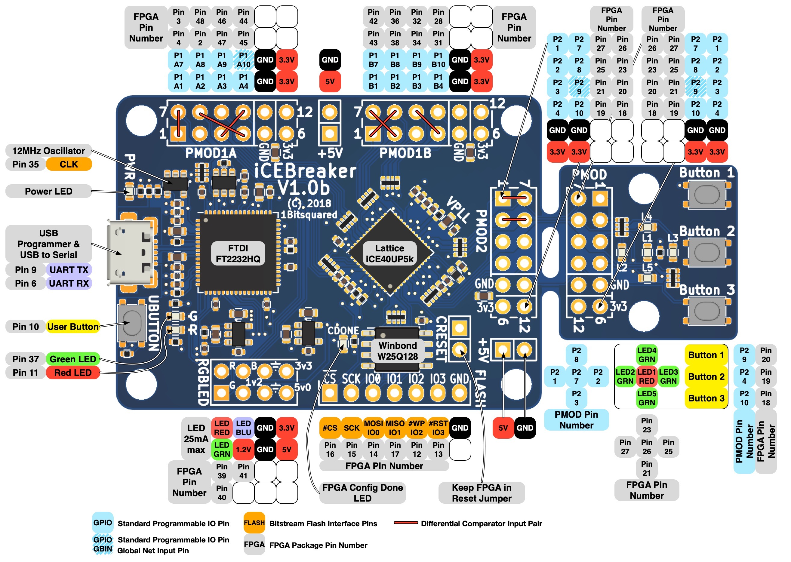
The pinout on https://raw.githubusercontent.com/icebreaker-fpga/icebreaker/master/img/icebreaker-v1_0b-legend.jpg is wrong for the SPI header. FPGA pin number for IO0 and IO1 are swapped.
Hello. I saw several projects aiming to integrate softcore to Arduino IDE in a way that the FPGA can then be programmed in C quite easily without much user setup.
For example the lattuino project:
http://fpgalibre.sourceforge.net/Lattuino_en/index.html#tp2
https://github.com/INTI-CMNB/Lattuino_IP_Core
https://github.com/INTI-CMNB/AVR_for_iCE40_IP_Core
Or the FPGArduino:
http://www.nxlab.fer.hr/fpgarduino/
https://github.com/f32c/f32c
Do you think, you can provide such support for icebreaker board? (doesn't need to be AVR, might as well be RISC-V)
I fully understand the difference between programming FPGA in HDL and programming softcore in C. But i think such integration would be great showcase for beginners who come from arduino world to slowly ease into FPGA...
Thanks for considering this.
In "This impressive flexible design by Sylvain Munaut (a.k.a. tnt)"
please replace
https://github.com/smunaut/icebreaker-temp/tree/master/rgb_panel
with
https://github.com/smunaut/ice40-playground/tree/master/projects/rgb_panel
I have tested that code with my icebreaker, and it works as of today
if nothing else, adding the image below to the 'img' directory and the Readme will help. time to start the Wiki?

According to @jgmcc42 the 10K pullups are to weak for WS2812 protocol. They should be 1K.
This should be fixed in the schematics and the docs.
What is the frequency accuracy of the 12 MHz oscillator (U7) on the Icebreaker board?
The schematic does not define the part number, is a BOM available somewhere?
The 93C46B-SOT-23-6 IC VCC is rated at 5V. The correct version for 3V3 is the 93LC46B.

It turns out that we do not need to program the FTDI flash chip with anything. We can save a few placements and parts. Let's keep the footprints in case we find out that we need them in the future or the user decides to add that functionality for their own needs.
Close this issue when the schematic DNP fields are marked accordingly and the note about the circuit being optional is added to the schematic.
Please add the following feature:
CRESET_B on the FPGA and ADBUS7 on the FTDI.CRESET_B.I would have needed that a few times now when writing designs that talk to the flash, or use the flash io pins. When the design puts the flash in state where it is not responsive anymore, you need to find a way of preventing the FPGA from booting on power up or you cant reprogram the flash anymore.
Having SPI communication from host to the ice40 has many benefits :
The only thing needed is a way to differentiate between host accessing the flash and the host accessing the user logic in the fpga.
This can be done one of two ways :
So all in all, I think a solder jumper from LEDG to ADBUS3 would be a good idea.
I made a mistake when transcribing the pinout of the ice40up5k to the schematic symbol. The RGB2 should be RGB1 and vice versa.

Thanks to @arturo182 for pointing it out. ;)
I am currently, working on creating a BOM with MPN's and DigiKey part numbers.
Anyone wants to help?
Hello everyone. I'm going to start working with an FPGA of this kind in September, and I wanted to know if there is any external power pins to keep the board on without USB cable, and what is the power input consumption from the board. TIA
This is derived from the HyperRAM issue #7 we will have to rethink it's location and population status for the V2.0 hardware cycle.
It would be good to add a section on hardware hacking. Here's what I know of.
The WS2812 ear requires two 10K resistors in 0603 packages and a BSS138 MOSFET in SOT23 package. And a header.
The RGB LED pad fits a Cree CLX6F LED.
You can piggyback a QSPI RAM chip onto the flash chip and bring the CS pin out to the nearby pad. The suggested part is Lyontek LY68L6400. It is available from lcsc.com. The datasheet is here. http://esp32.de/lyontek/pSRAM/LY68L6400_0.3.pdf
I have an idea:
Add HyperBus RAM (selfrefresh DRAM) to design, its small, cheap, low pin count but enough fast , and enough space (8 or 16MB)
S27KL0641 or S27KS0641
http://www.cypress.com/products/hyperram-memory
https://www.digikey.com/en/product-highlight/c/cypress/hyperram-memory
it will be good for image prcessing/buffering etc.
Based on input from @mubes and @MarkusBec we should consider putting in some inline resistors for all the FPGA IO pins. This is necessary to allow for high speed communications.
It is not always clear for everyone what COPI/CIPO stands for.
This should be added to the schematics to avoid ambiguity.
For additional information refer to the OSHWA resolution.
All in title : Would be nice to have a physical button.
We need to add easily accessible USB pads on the reverse side of the iCEBreaker. At least on the bitsy version of the board. The pads should be similar if not the same as the ones on the 1Bitsy boards. It will make debugging of the @tinyfpga bootloader much easier, and allow the user to solder in a USB cable if necessary.
I have chosen better buttons for the icebreaker. They have a better feel and are more affordable.
The new button and footprint can be found on Aliexpress.


They fit on the current footprint but it is not perfectly matching the pins of the new button.
Red and blue are swapped on the RGB LED symbol. Red should be between pins 3 and 4, blue should be between pins 1 and 6.
The AUX CS jumper can be closed to connect the first FTDI channel (used normally for bitstream flash or FPGA SRAM programming) to the FPGA Red LED pin. This jumper allows us to stream SPI data into the FPGA resuing the programming port after the programming is done.
One current example using this system is driving LED panels using the @smunaut rgb_panel design. Also the project SLED out_mpsse_spi module supports this protocol and can be used as a data source.
Several of us have now used our iCEBreakers with the jumper set, and it does not seem to interfere with any normal operation of the board even if not in use. To make things easier for the users that want to quickly play around with LED panels we should change the NO jumper to NC. This will allow for separation of this connection if some issue appears down the road.
Greetings folks, I would like to make a suggestion. I can turn this into a PR if there is interest.
The FT2232H has as regulated 1.8V output. VCCIO2 provides a jumper for supplying a different IO voltage. Wouldn't it be nice if +1V8 could be optionally used to power VCCIO2? For example, there are a number of single board computers with 1.8V GPIO and I2S, it would be nice to be able to connect the icebreaker PMOD to them directly.
I believe that powering VCCIO2 from FT2232H VREGOUT would be compatible with the UP5K power sequencing requirements.
I can see two ways to make this happen:
To show what I mean, for option (1) here is how it could work:
Add test point:

On F.Cu, add via to route +1V8 to B.Cu:

Add pad to B.Cu:

A declarative, efficient, and flexible JavaScript library for building user interfaces.
🖖 Vue.js is a progressive, incrementally-adoptable JavaScript framework for building UI on the web.
TypeScript is a superset of JavaScript that compiles to clean JavaScript output.
An Open Source Machine Learning Framework for Everyone
The Web framework for perfectionists with deadlines.
A PHP framework for web artisans
Bring data to life with SVG, Canvas and HTML. 📊📈🎉
JavaScript (JS) is a lightweight interpreted programming language with first-class functions.
Some thing interesting about web. New door for the world.
A server is a program made to process requests and deliver data to clients.
Machine learning is a way of modeling and interpreting data that allows a piece of software to respond intelligently.
Some thing interesting about visualization, use data art
Some thing interesting about game, make everyone happy.
We are working to build community through open source technology. NB: members must have two-factor auth.
Open source projects and samples from Microsoft.
Google ❤️ Open Source for everyone.
Alibaba Open Source for everyone
Data-Driven Documents codes.
China tencent open source team.
